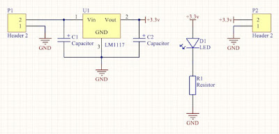
Altium Schematic To Pcb
Altium schematic lm386 Altium schematic trouble pcb between Design pcb schematic and layout in altium by sociallyvegan
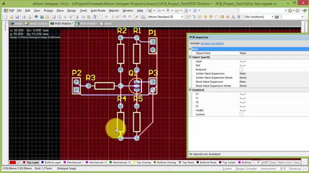
Altium PCB design - Electrical Engineering Stack Exchange
Altium designer tutorial: schematic, pcb library and pcb project 5 Altium how to make it to follow net connection order.. Tutorial schematic altium pcb designer embedded engineering system continue layout next make will
Altium pcb github layout issus footprint resistor
1 hour tour about altium designer(schematic-pcb designing)Embedded system engineering: altium designer tutorial 3 Design pcb schematic and layout in altium by sociallyveganScheme pcb altium please help errors guess there.
Altium pcb designAltium designer 20.2.3 crack + serial key free download [2020] Schematic altium pcb fiverr screenDesign schematics and pcb in altium by faiz07.

Pcb altium
Altium 17 create pcb from schematicHelp please with altium scheme in pcb. : printedcircuitboard Altium pcb designer tutorial library schematic projectResistor array footprint altium.
Altium schematics fiverr screenAltium trouble between schematic and pcb design Altium fiverrPcb altium schematic alliance create solutions portfolio.

How to create a pcb schematic
Altium pcbAltium schematic connection follow order make wires pcb How to create a pcb schematicAltium designer key serial schematic pcb crack.
Design schematic and pcb in altium by wangdegangAltium fiverr .


![Altium Designer 20.2.3 Crack + Serial Key Free Download [2020]](https://i2.wp.com/resources.altium.com/sites/default/files/inline-images/migrate/aHViPTY1NjQ2JmNtZD1pdGVtZWRpdG9yaW1hZ2UmZmlsZW5hbWU9aXRlbWVkaXRvcmltYWdlXzVhYjU1ZjkxYjliMzYucG5nJnZlcnNpb249MDAwMCZzaWc9M2E4MzNiMDgzNzBjZDQxOWMxNjc0NDU2MGM0NTc5ZTY%25253D)


